Wednesday, April 3rd, 2024
ECS154A Lecture: logic gates, SOP
- how to implement FISC on hardware level?
- CPU cycle: fetch decode execute write-back
- fetch: reading the instruction(s) from main memory
- decode: parse the opcode & operands & determine the semantics of the instruction
- execute: actually execute the parsed instruction
- write-back: save any computation result to relevant registers or memory
- for FISC, instruction memory (IM) is 8-bit wide (each instruction is capped to 8 bits)
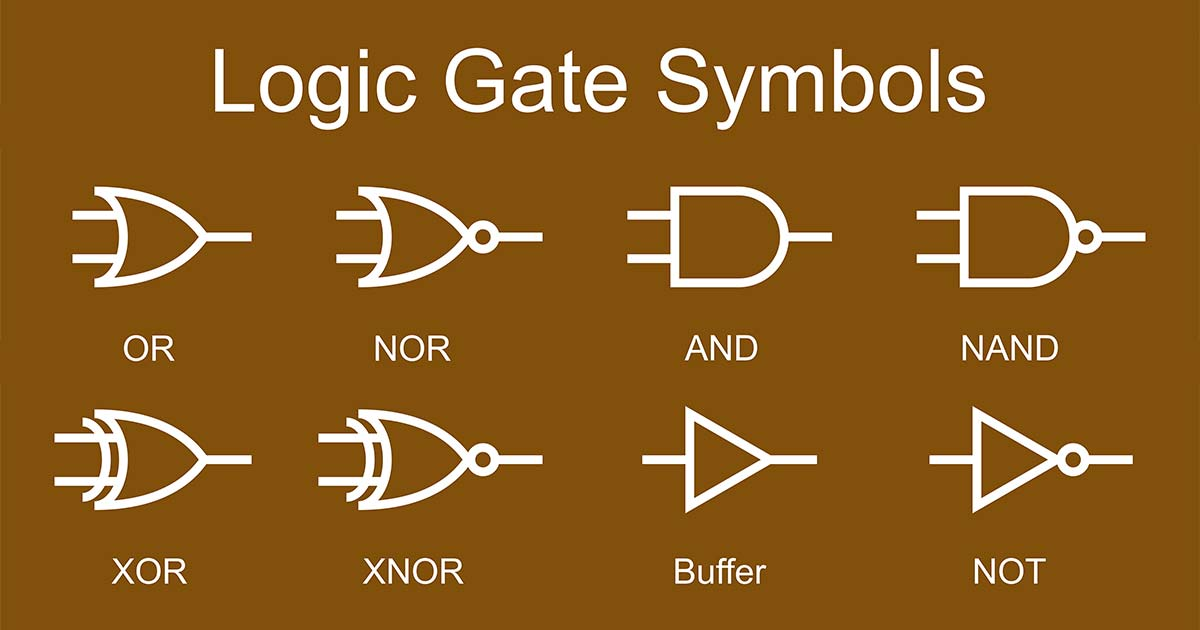
- in gates, circle = inverter

without circle = buffer
write truth table in canonical form (lowest possible truth value first, e.g., 00, 01, 10, 11)
note how inverter (circle) is at the end; apply inversion after the base operation (e.g., NOR = do OR then NOT the result)
exclusion is applied before the base operation, so if both inputs are 1, the result is 0
gates that have the same outputs are considered the same, so there are 4 possible one-input gate (truth table has 2 rows)
perspectives of digital logic
- product-of-sum (POS): doesn’t matter for this class
- sum-of-product (SOP): use ors of ands to represent a digital logic
- each True row in the truth table is turned into a product, so if A = 0 & B = 1 outputs 1, then it’s . add them together to form the expression for the logic
- can be used to turn an truth table to a schematic made of AND and OR gates