Metadata
- File: Digital design and computer architecture by Harris et al (2016).pdf; Digital design and computer architecture by Harris et al (2016).pdf
- Zotero: View Item
- Type: Book
- Title: Digital design and computer architecture,
- Author: Harris, Sarah L.; Harris, David Money;
- Publisher: Elsevier, Morgan Kaufmann,
- Location: Amsterdam Boston Heidelberg,
- Year: 2016
- ISBN: 978-0-12-800056-4
Abstract
Digital Design and Computer Architecture, Second Edition, takes a unique and modern approach to digital design, introducing the reader to the fundamentals of digital logic and then showing step by step how to build a MIPS microprocessor in both Verilog and VHDL. This new edition combines an engaging and humorous writing style with an updated and hands-on approach to digital design. It presents new content on I/O systems in the context of general purpose processors found in a PC as well as microcontrollers found almost everywhere. Beginning with digital logic gates and progressing to the design of combinational and sequential circuits, the book uses these fundamental building blocks as the basis for the design of an actual MIPS processor. It provides practical examples of how to interface with peripherals using RS232, SPI, motor control, interrupts, wireless, and analog-to-digital conversion. SystemVerilog and VHDL are integrated throughout the text in examples illustrating the methods and techniques for CAD-based circuit design. There are also additional exercises and new examples of parallel and advanced architectures, practical I/O applications, embedded systems, and heterogeneous computing, plus a new appendix on C programming to strengthen the connection between programming and processor architecture. This new edition will appeal to professional computer engineers and to students taking a course that combines digital logic and computer architecture. - Review: “…intended as a course text for college or university level students, this book would serve just as well for anyone who just wants to learn about computer architecture or design… it stands as one of the best introductions to the subject and seems ideal for anyone wanting to learn digital design with no prior knowledge. The time investment would be handsomely rewarded and the range of topics covered, as well as the clear explanation of trickier issues, is extremely impressive.” — BCS.org, April 2013 “Harris and Harris have taken the popular pedagogy from Computer Organization and Design down to the next level of refinement, showing in detail how to build a MIPS microprocessor in both Verilog and VHDL. Given the exciting opportunity that students have to run large digital designs on modern FGPAs, the approach the authors take in this book is both informative and enlightening.” —David A. Patterson, University of California at Berkeley, Co-author of Computer Organization and Design “Developed at Harvey Mudd College, this undergraduate textbook introduces combinatorial logic and sequential logic circuit design, describes the computer’s microarchitecture that connects hardware with software, and explains how to build a MIPS microprocessor.” — Reference and Research Book News, February 2013
Tags and Collections
- Keywords: 03 In Progress; Computer Architecture; Digital Logic; ECS154A; Textbook
Comments
Annotations
Annotations(4/24/2024, 12:31:52 AM)
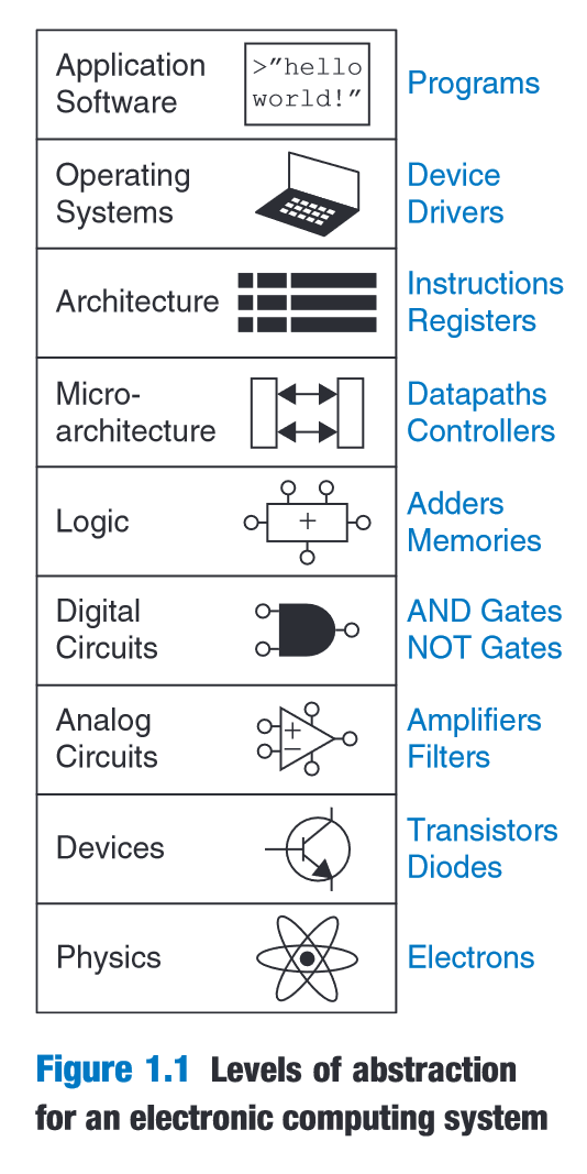
“Microarchitecture links the logic and architecture levels of abstraction.” (Harris and Harris, 2016, p. 15)
“The architecture level of abstraction describes a computer from the programmer’s perspective.” (Harris and Harris, 2016, p. 15)
 (Harris and Harris, 2016, p. 15)
 (Harris and Harris, 2016, p. 17)
“Microprocessors handle data in chunks called words. The size of a word depends on the architecture of the microprocessor.” (Harris and Harris, 2016, p. 24)
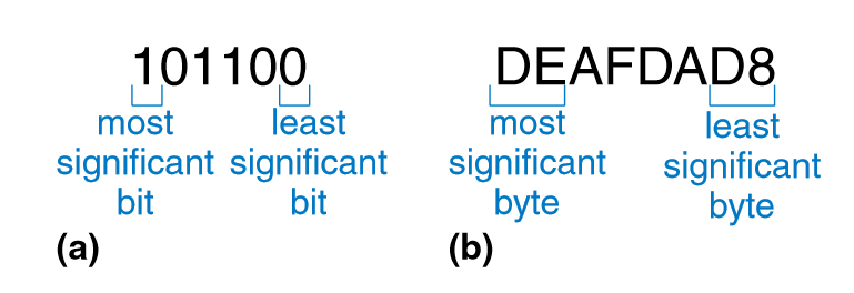
“Within a group of bits, the bit in the 1’scolumniscalledtheleast significant bit (lsb), and the bit at the other end is called the most significant bit (msb)” (Harris and Harris, 2016, p. 24)
 (Harris and Harris, 2016, p. 25)
“When a two’s complement number is extended to more bits, the sign bit must be copied into the most significant bit positions. This process is called sign extension.” (Harris and Harris, 2016, p. 29)
“Logic gates are simple digital circuits that take one or more binary inputs and produce a binary output.” (Harris and Harris, 2016, p. 30)
“the buffer might have desirable characteristics such as the ability to deliver large amounts of current to a motor or the ability to quickly send its output to many gates. This is an example of why we need to consider multiple levels of abstraction to fully understand a system; the digital abstraction hides the real purpose of a buffer.” (Harris and Harris, 2016, p. 31)
“An N-input XOR gate is sometimes called a parity gate and produces a TRUE output if an odd number of inputs are TRUE.” (Harris and Harris, 2016, p. 32)
“Suppose the lowest voltage in the system is 0 V, also called ground or GND. The highest voltage in the system comes from the power supply and is usually called VDD” (Harris and Harris, 2016, p. 33)
“The mapping of a continuous variable onto a discrete binary variable is done by defining logic levels” (Harris and Harris, 2016, p. 33)
“The first gate is called the driver and the second gate is called the receiver.” (Harris and Harris, 2016, p. 33)
“If the output of the driver is to be correctly interpreted at the input of the receiver, we must choose VOL < VIL and VOH > VIH.” (Harris and Harris, 2016, p. 34)
“The noise margin is the amount of noise that could be added to a worst-case output such that the signal can still be interpreted as a valid input.” (Harris and Harris, 2016, p. 34)
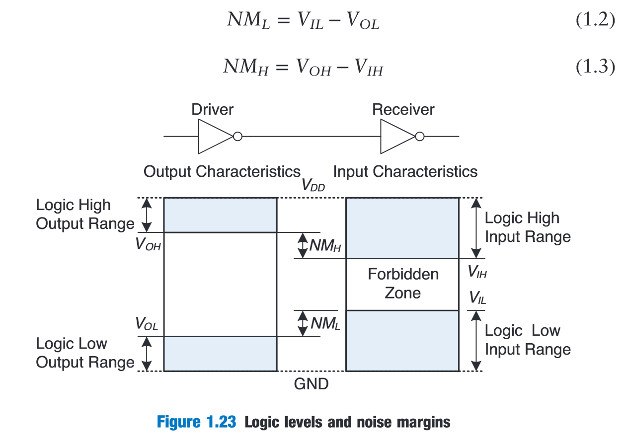 (Harris and Harris, 2016, p. 34)
Noise margin accounts for any noise on the path between the driver’s output and the receiver’s input.**
“The DC transfer characteristics of a gate describe the output voltage as a function of the input voltage when the input is changed slowly enough that the output can keep up.” (Harris and Harris, 2016, p. 35)
“A reasonable place to choose the logic levels is where the slope of the transfer characteristic dV(Y) /dV(A)is−1. These two points are called the unitygainpoints” (Harris and Harris, 2016, p. 35)
“digital logic gates are designed to conform to the static discipline. The static discipline requires that, given logically valid inputs, every circuit element will produce logically valid outputs.” (Harris and Harris, 2016, p. 35)
“gates are grouped into logic families such that all gates in a logic family obey the static discipline when used with other gates in the family” (Harris and Harris, 2016, p. 36)
“A circuit can be viewed as a black box, shown in Figure 2.1, with ▶ one or more discrete-valued input terminals ▶ one or more discrete-valued output terminals ▶ a functional specification describing the relationship between inputs and outputs ▶ a timing specification describing the delay between inputs changing and outputs responding.” (Harris and Harris, 2016, p. 65)
“Peering inside the black box, circuits are composed of nodes and elements. An element is itself a circuit with inputs, outputs, and a specification. A node is a wire, whose voltage conveys a discrete-valued variable.” (Harris and Harris, 2016, p. 65)
“Digital circuits are classified as combinational or sequential. Acombinational circuit’s outputs depend only on the current values of the inputs” (Harris and Harris, 2016, p. 66)
“A sequential circuit’s outputs depend on both current and previous values of the inputs” (Harris and Harris, 2016, p. 66)
“A combinational circuit is memoryless, but a sequential circuit has memory” (Harris and Harris, 2016, p. 66)
“To simplify drawings, we often use a single line with a slash through it and a number next to it to indicate a bus, a bundle of multiple signals.” (Harris and Harris, 2016, p. 66)
“A circuit is combinational if it consists of interconnected circuit elements such that ▶ Every circuit element is itself combinational. ▶ Every node of the circuit is either designated as an input to the circuit or connects to exactly one output terminal of a circuit element. ▶ The circuit contains no cyclic paths: every path through the circuit visits each circuit node at most once.” (Harris and Harris, 2016, p. 67)
“We call A the true form of the variable and A the complementary form;” (Harris and Harris, 2016, p. 68)
“The AND of one or more literals is called a product or an implicant” (Harris and Harris, 2016, p. 68)
“A minterm is a product involving all of the inputs to the function” (Harris and Harris, 2016, p. 68)
“Similarly, the OR of one or more literals is called a sum” (Harris and Harris, 2016, p. 68)
“A maxterm is a sum involving all of the inputs to the function” (Harris and Harris, 2016, p. 68)
“This is called the sum-of-products canonical form of a function because it is the sum (OR) of products (ANDs forming minterms).” (Harris and Harris, 2016, p. 69)
“An alternative way of expressing Boolean functions is the productof-sums canonical form. Each row of a truth table corresponds to a maxterm that is FALSE for that row.” (Harris and Harris, 2016, p. 70)
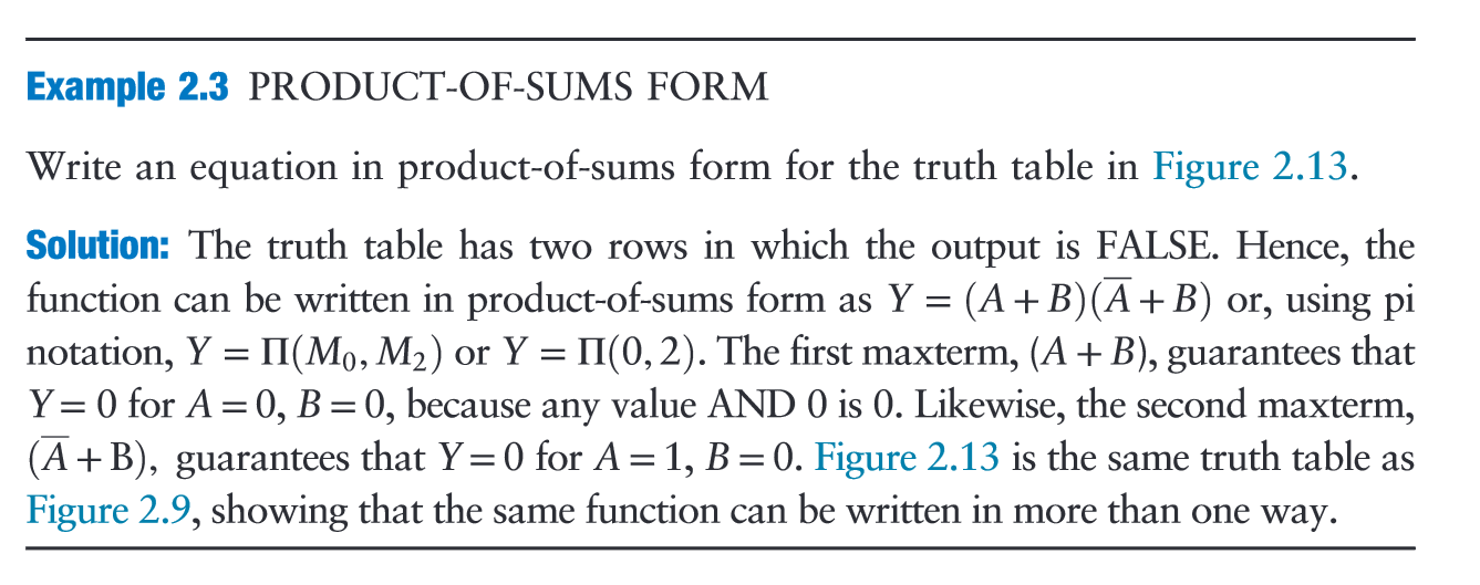 (Harris and Harris, 2016, p. 70)
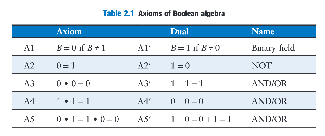
“Axioms and theorems of Boolean algebra obey the principle of duality. If the symbols 0 and 1 and the operators • (AND) and + (OR) are interchanged, the statement will still be correct.” (Harris and Harris, 2016, p. 71)
 (Harris and Harris, 2016, p. 71)
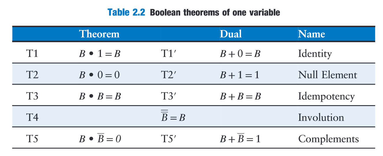
“Involution, T4, is a fancy way of saying that complementing a variable twice results in the original variable.” (Harris and Harris, 2016, p. 72)
 (Harris and Harris, 2016, p. 72)
 (Harris and Harris, 2016, p. 73)
“proofs of theorems with a finite number of variables are easy: just show that the theorem holds for all possible values of these variables. This method is called perfect induction and can be done with a truth table” (Harris and Harris, 2016, p. 74)
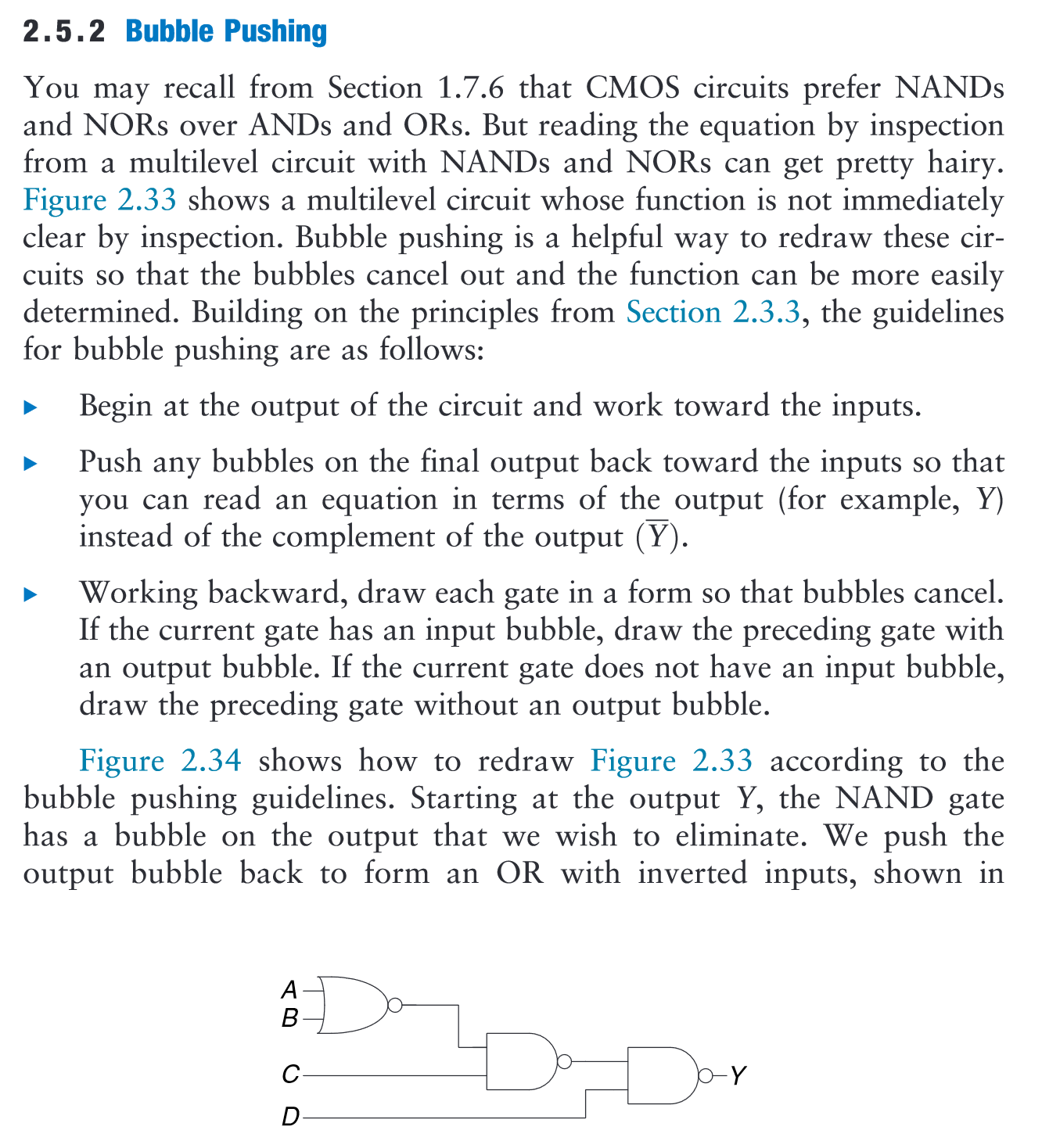
“By drawing schematics in a consistent fashion, we make them easier to read and debug. We will generally obey the following guidelines: ▶ Inputs are on the left (or top) side of a schematic. ▶ Outputs are on the right (or bottom) side of a schematic. ▶ Whenever possible, gates should flow from left to right. ▶ Straight wires are better to use than wires with multiple corners (jagged wires waste mental effort following the wire rather than thinking of what the circuit does). ▶ Wires always connect at a T junction. ▶ A dot where wires cross indicates a connection between the wires. ▶ Wires crossing without a dot make no connection.” (Harris and Harris, 2016, p. 77)
“Any Boolean equation in sum-of-products form can be drawn as a schematic in a systematic way similar to Figure 2.23. First, draw columns for the inputs. Place inverters in adjacent columns to provide the complementary inputs if necessary. Draw rows of AND gates for each of the minterms. Then, for each output, draw an OR gate connected to the minterms related to that output. This style is called a programmable logic array (PLA)” (Harris and Harris, 2016, p. 77)
 (Harris and Harris, 2016, p. 81)
“Figure 2.39 shows a case where node Y is driven both HIGH and LOW. This situation, called contention” (Harris and Harris, 2016, p. 83)
“The outputs are called one-hot, because exactly one is “hot” (HIGH) at a given time.” (Harris and Harris, 2016, p. 96)
“The propagation delay tpd is the maximum time from when an input changes until the output or outputs reach their final value.” (Harris and Harris, 2016, p. 98)
“The contamination delay tcd is the minimum time from when an input changes until any output starts to change its value.” (Harris and Harris, 2016, p. 98)
“The critical path, shown in blue, is the path from input A or B to output Y.” (Harris and Harris, 2016, p. 99)
“The short path through the circuit, shown in gray, is from input D to output Y. This is the shortest, and therefore the fastest, path through the circuit” (Harris and Harris, 2016, p. 100)
“The propagation delay of a combinational circuit is the sum of the propagation delays through each element on the critical path. The contamination delay is the sum of the contamination delays through each element on the short path.” (Harris and Harris, 2016, p. 100)
“it is possible that a single input transition can cause multiple output transitions. These are called glitches or hazards.” (Harris and Harris, 2016, p. 102)
“if the circuitry implementing one of the prime implicants turns off before the circuitry of the other prime implicant can turn on, there is a glitch. To fix this, we add another circle that covers that prime implicant boundary, as shown in Figure 2.78.” (Harris and Harris, 2016, p. 104)
“Because the vast majority of interesting systems have simultaneous (or nearsimultaneous) transitions on multiple inputs, glitches are a fact of life in most circuits.” (Harris and Harris, 2016, p. 105)
“The fundamental building block of memory is a bistable element, an element with two stable states.” (Harris and Harris, 2016, p. 118)
“A subtle point is that the circuit has a third possible state with both outputs approximately halfway between 0 and 1. This is called a metastable state” (Harris and Harris, 2016, p. 119)
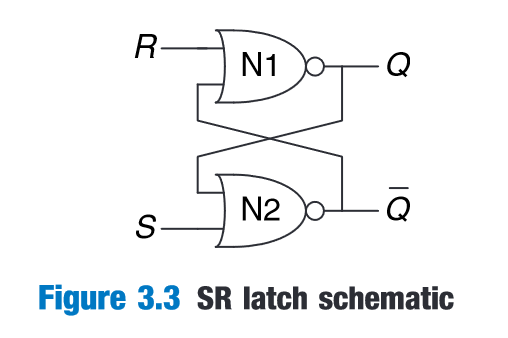 (Harris and Harris, 2016, p. 120)
 (Harris and Harris, 2016, p. 121)
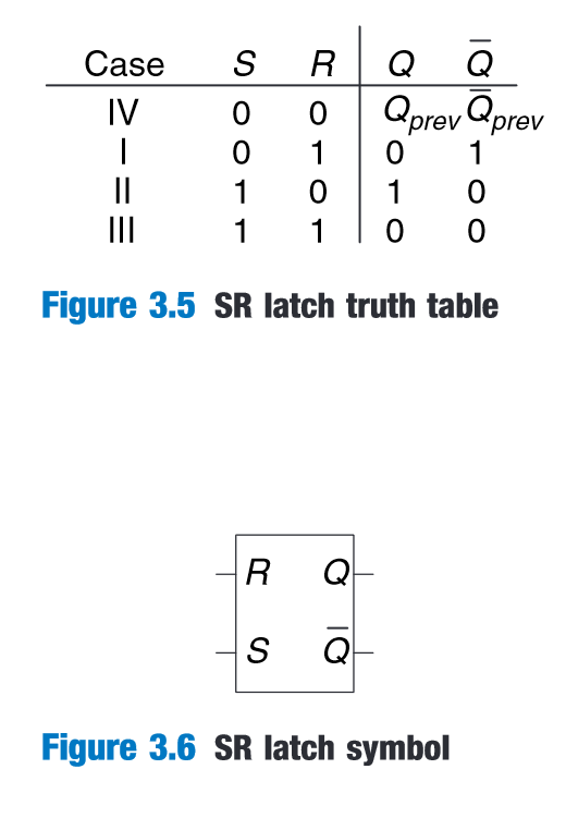
SR latch truth table & symbol**
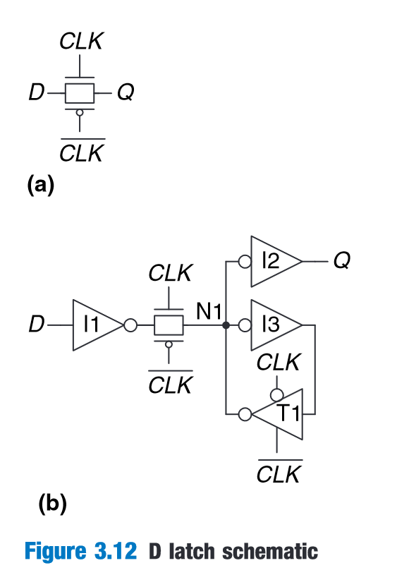
“The D latch in Figure 3.7(a) solves these problems. It has two inputs. The data input, D, controls what the next state should be. The clock input, CLK, controls when the state should change.” (Harris and Harris, 2016, p. 122)
“When CLK = 1, the latch is transparent.The data at D flows through to Q as if the latch were just a buffer. When CLK = 0, the latch is opaque.” (Harris and Harris, 2016, p. 122)
“D latch is sometimes called a transparent latch or a level-sensitive latch.” (Harris and Harris, 2016, p. 122)
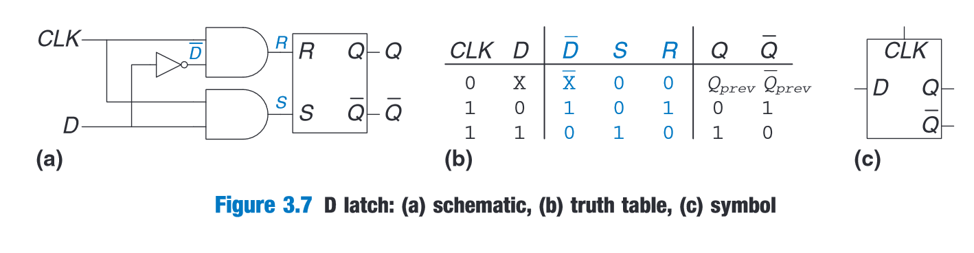 (Harris and Harris, 2016, p. 122)
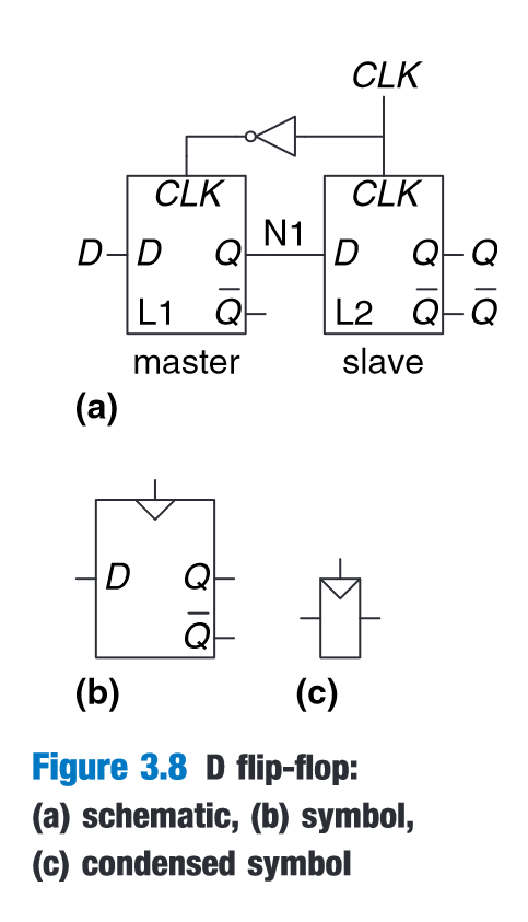
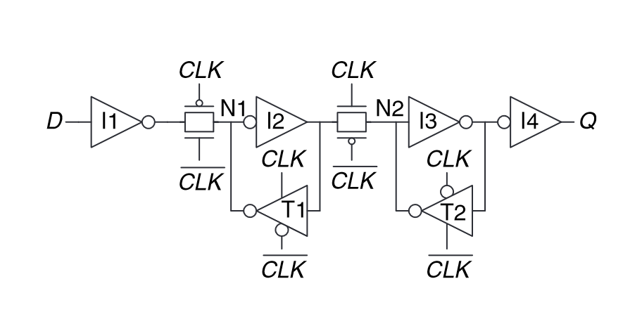
“A D flip-flop can be built from two back-to-back D latches controlled by complementary clocks, as shown in Figure 3.8(a). The first latch, L1, is called the master. The second latch, L2, is called the slave.” (Harris and Harris, 2016, p. 123)
“a D flip-flop copies D to Q on the rising edge of the clock, and remembers its state at all other times.” (Harris and Harris, 2016, p. 123)
“A D flip-flop is also known as a master-slave flip-flop,anedge-triggered flip-flop,orapositive edge-triggered flip-flop.” (Harris and Harris, 2016, p. 123)
 (Harris and Harris, 2016, p. 123)
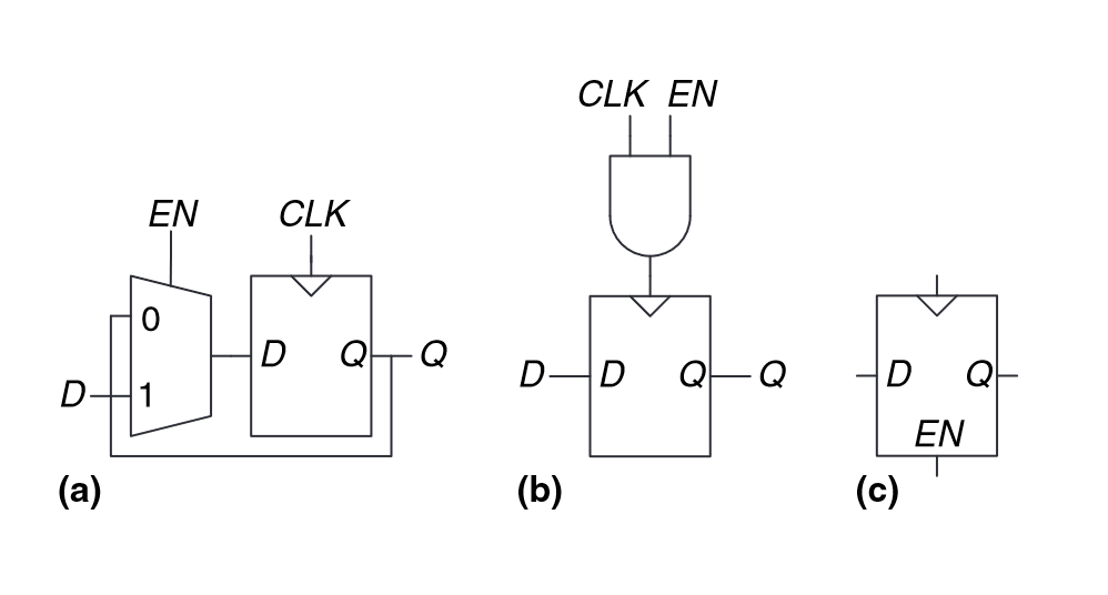
“An enabled flip-flop adds another input called EN or ENABLE to determine whether data is loaded on the clock edge. When EN is TRUE, the enabled flip-flop behaves like an ordinary D flip-flop. When EN is FALSE, the enabled flip-flop ignores the clock and retains its state.” (Harris and Harris, 2016, p. 124)
 (Harris and Harris, 2016, p. 124)
 (Harris and Harris, 2016, p. 124)
enabled flip-flop via (a) multiplexer or (b) gated design**
“Generally, performing logic on the clock is a bad idea.” (Harris and Harris, 2016, p. 125)
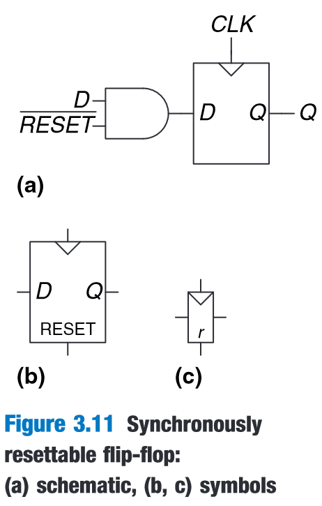
“A resettable flip-flop adds another input called RESET.WhenRESET is FALSE, the resettable flip-flop behaves like an ordinary D flip-flop. When RESET is TRUE, the resettable flip-flop ignores D and resets the output to 0.” (Harris and Harris, 2016, p. 125)
 (Harris and Harris, 2016, p. 125)
synchronously resettable flip-flop**
 (Harris and Harris, 2016, p. 126)
3.12 compact D latch schematic**
 (Harris and Harris, 2016, p. 126)
“loops called cyclic paths,in which outputs are fed directly back to inputs” (Harris and Harris, 2016, p. 129)
“designers break the cyclic paths by inserting registers somewhere in the path” (Harris and Harris, 2016, p. 129)
“The registers contain the state of the system, which changes only at the clock edge, so we say the state is synchronized to the clock. If the clock is sufficiently slow, so that the inputs to all registers settle before the next clock edge, all races are eliminated.” (Harris and Harris, 2016, p. 130)
“The rules of synchronous sequential circuit composition teach us that a circuit is a synchronous sequential circuit if it consists of interconnected circuit elements such that ▶ Every circuit element is either a register or a combinational circuit ▶ At least one circuit element is a register ▶ All registers receive the same clock signal ▶ Every cyclic path contains at least one register.” (Harris and Harris, 2016, p. 130)
“These forms are called finite state machines (FSMs). They get their name because a circuit with k registers can be in one of a finite number (2k) of unique states.” (Harris and Harris, 2016, p. 132)
“In Moore machines, the outputs depend only on the current state of the machine.” (Harris and Harris, 2016, p. 132)
“In Mealy machines, the outputs depend on both the current state and the current inputs.” (Harris and Harris, 2016, p. 132)
“3.4.1 FSM Design Example” (Harris and Harris, 2016, p. 132)
“Ben’s next step is to sketch the state transition diagram, shown in Figure 3.25, to indicate all the possible states of the system and the transitions between these states.” (Harris and Harris, 2016, p. 133)
“The arc labeled Reset pointing from outer space into state S0 indicates that the system should enter that state upon reset, regardless of what previous state it was in.” (Harris and Harris, 2016, p. 134)
“state transition table (Table 3.1), which indicates, for each state and input, what the next state, S′, should be.” (Harris and Harris, 2016, p. 134)
“To build a real circuit, the states and outputs must be assigned binary encodings.” (Harris and Harris, 2016, p. 134)
“Similarly, Ben writes an output table (Table 3.5) indicating, for each state, what the output should be in that state.” (Harris and Harris, 2016, p. 136)
“it is often possible to choose a good encoding by inspection, so that related states or outputs share bits.” (Harris and Harris, 2016, p. 138)
“With binary encoding, as was used in the traffic light controller example, each state is represented as a binary number. Because K binary numbers can be represented by log2K bits, a system with K states only needs log2K bits of state.” (Harris and Harris, 2016, p. 138)
“In one-hot encoding, a separate bit of state is used for each state.” (Harris and Harris, 2016, p. 138)
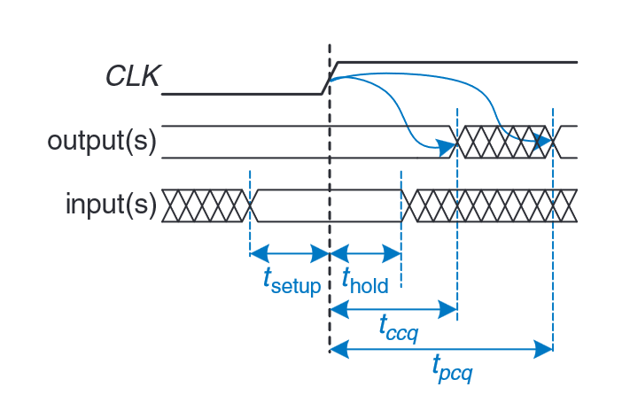
“Recall that a flip-flop copies the input D to the output Q on the rising edge of the clock. This process is called sampling D on the clock edge. If D is stable at either 0 or 1 when the clock rises, this behavior is clearly defined.” (Harris and Harris, 2016, p. 150)
“Similarly, a sequential element has an aperture time around the clock edge, during which the input must be stable for the flip-flop to produce a well-defined output. The aperture of a sequential element is defined by a setup time and a hold time, before and after the clock edge, respectively.” (Harris and Harris, 2016, p. 150)
“the dynamic discipline limits us to using signals that change outside the aperture time” (Harris and Harris, 2016, p. 150)
“Hence, we can simply write A[n], the value of signal A at the end of the nth clock cycle, where n is an integer” (Harris and Harris, 2016, p. 150)
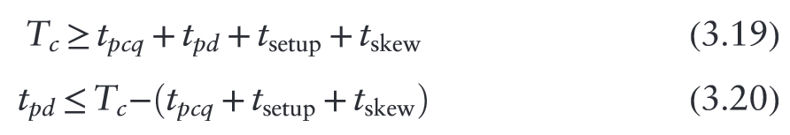
“In real systems, the clock does not reach all flip-flops at precisely the same time. This variation in time, called clock skew, further increases the necessary clock period.” (Harris and Harris, 2016, p. 150)
“For the circuit to sample its input correctly, the input (or inputs) must have stabilized at least some setup time, tsetup, before the rising edge of the clock and must remain stable for at least some hold time, thold, after the rising edge of the clock. The sum of the setup and hold times is called the aperture time of the circuit, because it is the total time for which the input must remain stable.” (Harris and Harris, 2016, p. 151)
“The dynamic discipline states that the inputs of a synchronous sequential circuit must be stable during the setup and hold aperture time around the clock edge.” (Harris and Harris, 2016, p. 151)
“The clock period or cycle time, Tc, is the time between rising edges of a repetitive clock signal. Its reciprocal, fc = 1/Tc, is the clock frequency.” (Harris and Harris, 2016, p. 151)
 (Harris and Harris, 2016, p. 151)
3.37 timing specification for synchronous sequential circuit**
 (Harris and Harris, 2016, p. 152)
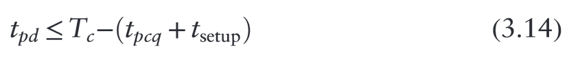
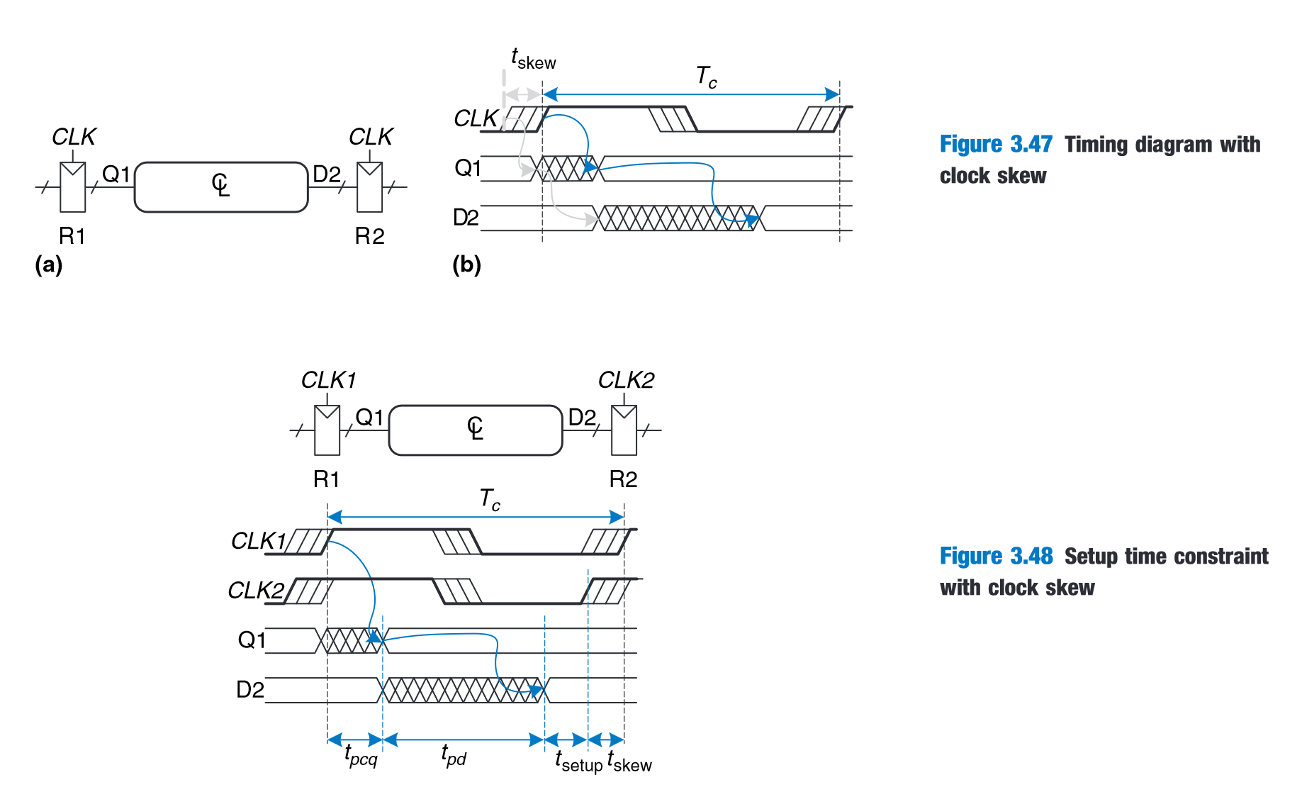
Clock period should be minimized such that it is equal to or barely greater than the sum of (1) clock signal-to-R1 register output time, (2) propagation delay of combinational logic element, and (3) setup time constraint of the next register.**
 (Harris and Harris, 2016, p. 152)
Setup time constraint / max-delay constraint. This shows the limit on the max propagation delay of combinational logic elements in a synchronous sequential circuit.**
“The term in parentheses, tpcq + tsetup , is called the sequencing overhead.” (Harris and Harris, 2016, p. 152)
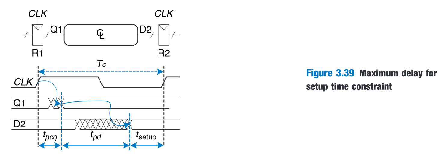 (Harris and Harris, 2016, p. 152)
3.39 maximum delay for setup time constraint **
 (Harris and Harris, 2016, p. 153)
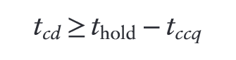
Hold time constraint. is the contamination delay between clock signal and the output of register R1. is the contamination delay of the combinational circuit’s output D. Since and are characteristics of the flip-flops, they are out of the circuit designer’s control, so the designer must ensure that the contamination delay of the circuit is great enough so that it only changes the output after the required hold time by the output register R2. Often, we can insert buffers to increase the contamination delay of the short paths to prevent a hold time violation as shown in the example at the end of 3.5.2.**
 (Harris and Harris, 2016, p. 153)
3.40 minimum delay / hold time constraint**
“In other words, a reliable flip-flop must have a hold time shorter than its contamination delay. Often, flip-flops are designed with thold = 0, so that Equation 3.17 is always satisfied.” (Harris and Harris, 2016, p. 154)
“hold time constraints are critically important. If they are violated, the only solution is to increase the contamination delay through the logic, which requires redesigning the circuit. Unlike setup time constraints, they cannot be fixed by adjusting the clock period.” (Harris and Harris, 2016, p. 154)
“The maximum delay constraint limits the number of consecutive gates on the critical path of a high-speed circuit, because a high clock frequency means a short clock period.” (Harris and Harris, 2016, p. 154)
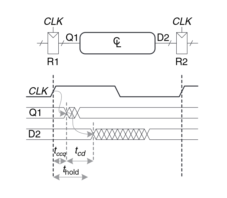
“This variation in clock edges is called clock skew. For example, the wires from the clock source to different registers may be of different lengths, resulting in slightly different delays” (Harris and Harris, 2016, p. 157)
“In the worst case, R1 receives the latest skewed clock and R2 receives the earliest skewed clock, leaving as little time as possible for data to propagate between the registers.” (Harris and Harris, 2016, p. 157)
 (Harris and Harris, 2016, p. 157)
3.46) CLK may arrive up to earlier.**
 (Harris and Harris, 2016, p. 158)
Now (after considering clock skew), the propagation delay of the circuit needs to be limited to what’s left of the clock period after taking away the clock-to-input (q), the setup constraint of output register R2, and the clock skew time.**
“In summary, clock skew effectively increases both the setup time and the hold time. It adds to the sequencing overhead, reducing the time available for useful work in the combinational logic. It also increases the required minimum delay through the combinational logic.” (Harris and Harris, 2016, p. 158)
 (Harris and Harris, 2016, p. 158)
“Three common CPA implementations are called ripple-carry adders, carry-lookahead adders, and prefix adders.” (Harris and Harris, 2016, p. 249)
“The ripplecarry adder has the disadvantage of being slow when N is large.” (Harris and Harris, 2016, p. 249)
 (Harris and Harris, 2016, p. 249)
 (Harris and Harris, 2016, p. 249)
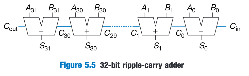 (Harris and Harris, 2016, p. 249)
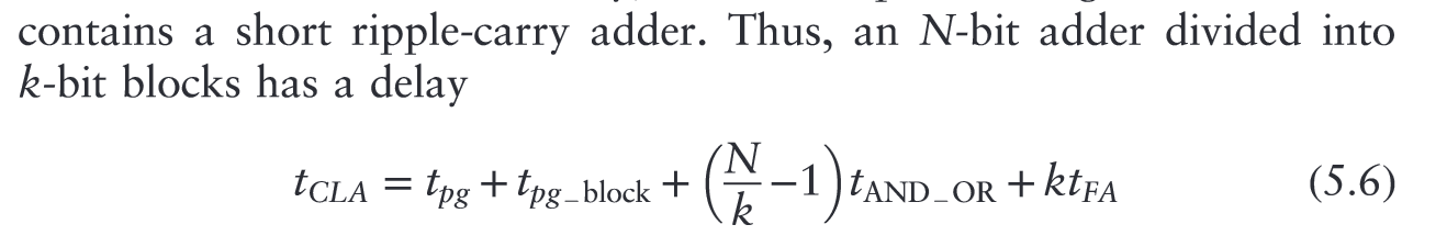 (Harris and Harris, 2016, p. 251)
N-bit CLA adder divided into k blocks has a delay defined by the above.**
 (Harris and Harris, 2016, p. 251)
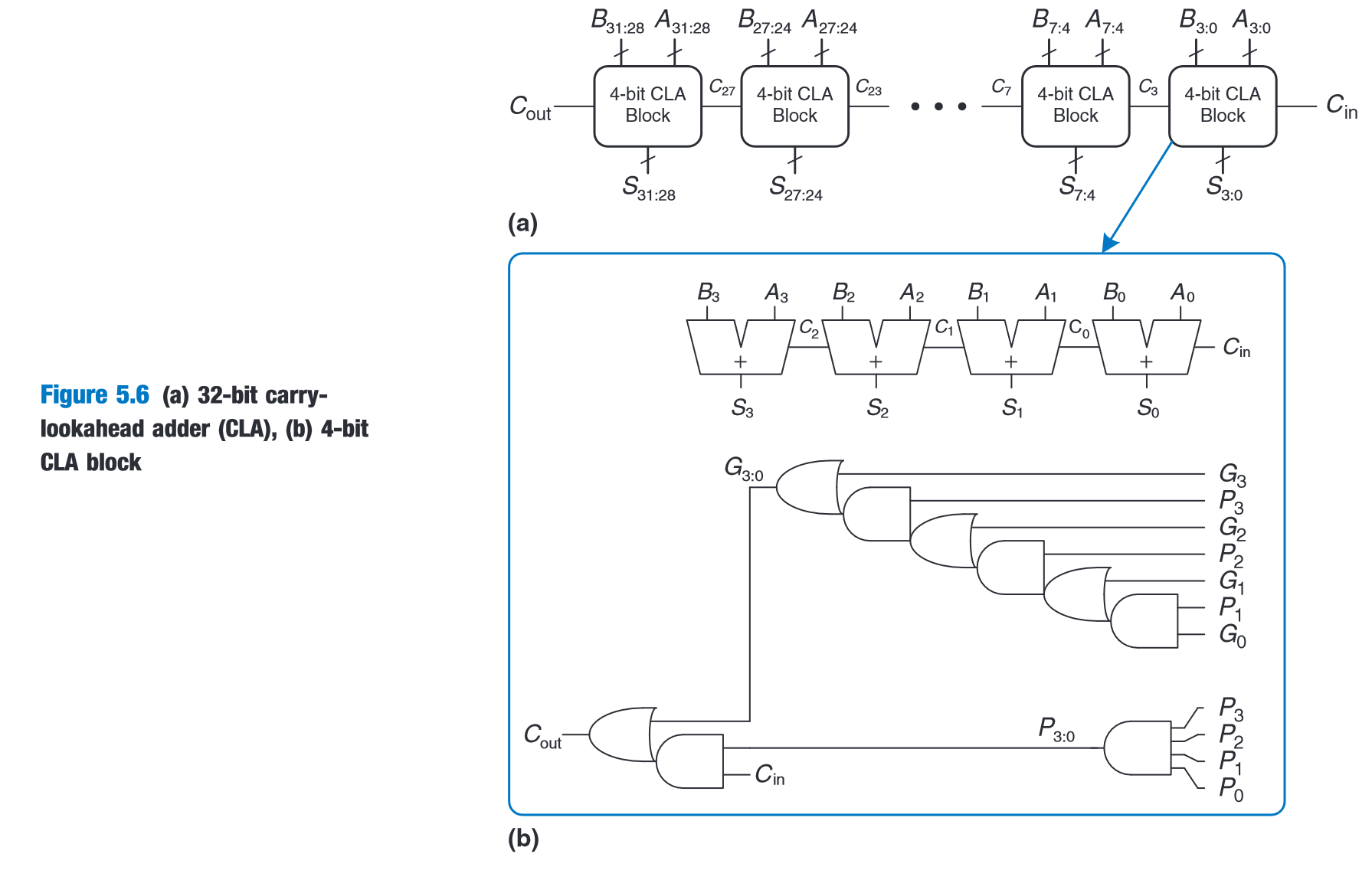
 (Harris and Harris, 2016, p. 258)
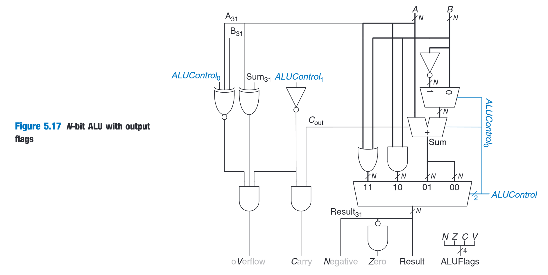
N-bit ALU with or, and, subtract, sum**
 (Harris and Harris, 2016, p. 259)
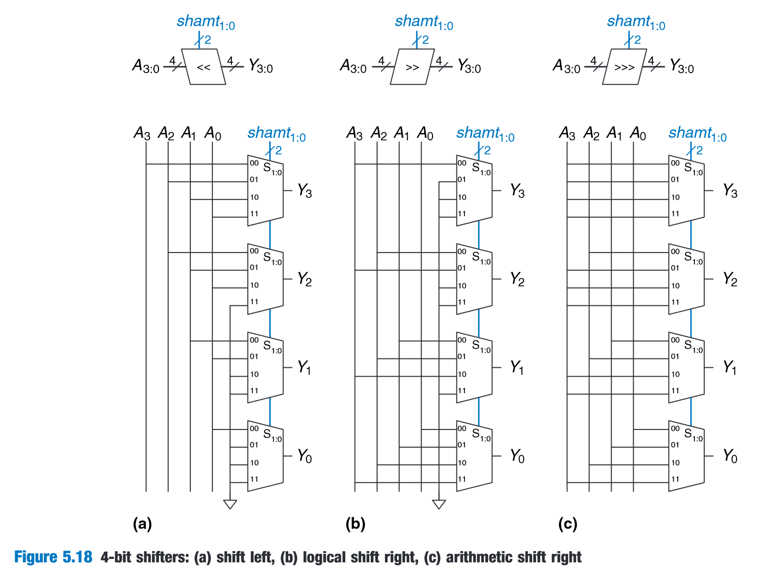
“The operators << , >>,and>>> typically indicate shift left, logical shift right, and arithmetic shift right, respectively.” (Harris and Harris, 2016, p. 260)
 (Harris and Harris, 2016, p. 261)
“The steps for adding floating-point numbers with the same sign are as follows: 1. Extract exponent and fraction bits. 2. Prepend leading 1 to form the mantissa. 3. Compare exponents. 4. Shift smaller mantissa if necessary. 5. Add mantissas. 6. Normalize mantissa and adjust exponent if necessary. 7. Round result. 8. Assemble exponent and fraction back into floating-point number.” (Harris and Harris, 2016, p. 268)
 (Harris and Harris, 2016, p. 269)
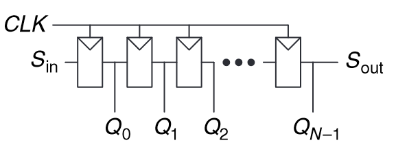
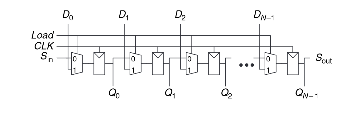
“A shift register has a clock, a serial input Sin, a serial output Sout ,andN parallel outputs QN−1:0, as shown in Figure 5.34. On each rising edge of the clock, a new bit is shifted in from Sin and all the subsequent contents are shifted forward. The last bit in the shift register is available at Sout. Shift registers can be viewed as serial-to-parallel converters.” (Harris and Harris, 2016, p. 270)
 (Harris and Harris, 2016, p. 270)
 (Harris and Harris, 2016, p. 271)
shift register with parallel load (parallel-to-serial converter)**